Sunday 15 July 2012


DAY 4- 10 JULY 2012
Morning Session
Assalamualaikum...
As usuall,my training day will started with update my blog first before proceed to training and learning session. But, unfortunately the internet connection here is always limited. After completed soldering process, it will continue with the test of circuit process. After complete soldering process, the PIC board will be tested by using vibration sensorand LCD to make sure it's well-function. The test is conducted using PIC C compiler software. Before the PIC board is test, coding must be done. The test is conducted to test :


i. power led

once we connect the circuit to the power supply,the power led will turn on.


ii. vibrator sensor

Ic that has been programmed must be attached on PIC board. After connect the vibrate sensor to the circuit, the vibrate sensor must be shake off to check the functionality of the circuit.


Once we shake the vibrate sensor,the led will turn on every time we shake the sensor.


iii. display  on LCD by activate relay


An IC also has been programmed with LCD coding functioning. Once we connect the circuit to LCD panel and turn on the circuit, the lcd will display a word "Hello Word" same as have been set in programming.


DAY 3- 9 JULY 2012
Assalamualaikum and Salam Sejahtera..
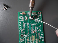
My task for today is continue with soldering process. The first thing I need to do is to soldered an SMD component first. Before starts to soldering process, we must know the procedure of surface mount components. A good eye, a steady hand and a soldering iron with a small, clean tip are required. We are using pin by pin method. This method are used for two pin components such as capacitor and resistor,small outline package and SOT

SMD Components Soldering  procedure
1)Place a small amount of solder on one of the two pads. Approximately 0.5mm in height.


2)   Grab the part with very fine tweezers. Bring the part overtop of the pads, slight to one side so that the part can sit flat against the PCB. Heat the pad already with solder and slide the part onto the pad so that it is centered between the pads. Remove heat.


 3)  Put a small force down on the part and re-heat the one pad to guarantee that the parts is flat against the PCB

4)     \Solder the other side of the part


5)      The solderings should not look like "round ball" on either side of the parts. If this is the cast, there is too much solder being appied to the joint. A properly soldered joint should have a curved line from the end of the pad to the top of the part.

SMD components that has been soldered


Through Hole Component Soldering Procedure
 1)After we prepare all components that we need to use for solder, we need to clean component lead and make sure it’s clean from dirt & smear.

2)Then we can insert the component and clinch lead. We need to cut off the excess wire first before we continued with soldering process

3) Next, we need to apply flux to soldering point. The purpose of applying flux to soldering point is to remove oxide layer from the base metal surface, to shield base metal surface from oxygen which re-oxidizemetal and to lower solder’s surface tension to improve wetting

4)Before soldering, we need to make sure that we are using only well-heated soldering iron. Clean soldering iron tip and then apply a bit of solder to iron tip. We need to ensure that solder are attached to tip.

5)In order to solder the point, we need to heat the soldering point first and soldering iron must contact both component lead and pcb copper.

6)Then apply solder wire and ensure that solder wire must contact both component lead and pcb copper.

7)Pull away soldering wire from solder point. Then pull away soldering iron from solder point when solder becomes shiny.

8)      During soldering process, the timing is important. Do not apply soldering iron too long or too short.

Complete

ACCEPTANCE CRITERIA OF SOLDERING
There is a criteria of good soldering that have been set up base on IPC-A-610 and J-STD-001 (Class 2)
Criteria:
•     Circumferential fillet and wetting= 270°
•     Percentage of PCB copper landarea covered with solder = 75%
•     Visible good wetting
•     Fillet Height = minimum ¼ Leadheight or 0.05mm
•     Lead height after cut =maximum 2.5mm
•     Solder finish = glossy or shinny
             Solder contact angle ≤90°
1


DAY 2 – 6 JULY 2012
Morning Session
I have attend an interview with company Recron (M) Sdn.Bhd that located at Nilai,Negeri Sembilan. After interview session and discuss their offer, I have made a decision to not accept their offer because the department and job they offer not have any related with my course. So, I decided to stay continue my industrial training under Utem Holding.
Afternoon Session
After coming back to Melaka, I have come back to UTEM. We were ask by Encik Mazran to create a blog for each of us as a journal during this practical period. He instructed us to update our blog with the things that we learn every single day. Then, he have give us a task schedule and a time table for us to followed . The task table is arrange as below:

MORNING

9.00am -10.00am : Report Blog
10.00am - 12.30pm : Daily Chores
1.00pm - 2.00pm : Break Time
2.00pm - 5.00pm : Daily Chores
5.00pm : Dismiss


TASK
MEMBERS
DURATION
All
Parallel [All Member]
Week 1 – Week 4
-          PCB/ Soldering
-          Sensor à Vibration
è Sonar
-          GSM Modem
PLC
Prequisite
Week 3
-          GSM Modem
BENT
Week 5
IP Camera
BENT student

Offline

Wifi

Mechanical Prototype

Week 6 - Week 10
PIC

PLC


Our first task at this new practical places is PCB soldering. The first thing we need to do is to soldered an SMD component first because this surface mount components are very small, and therefore special precautions (in additional to those required when working with through-hole components) must be taken.

The equipment that we will use are:
Solder Iron
Solder Paste
TGK-493 anti-static absorber (ionizer)
Tweezers
solder leads
Gripped board                                                                                                                              
And the components that we need to solder is:
Power and reset button
2 x GA 12 diode
PW LED and LED_C4
Resistor 2.2KΩ , 2 x 330Ω , 2 x 10kΩ  
Printed Circuit Board (PCB)
Capacitor 5 x 61µ 3

PCB Board


solder iron

Anti Static Absorber  
                        
Tweezers                                                    
solder paste
Solder Leads

Monday 9 July 2012


Day 1 (5 JULY 2012)
Assalamualaikum and Salam Sejahtera....
First of all,  I would like to thank a lot to Mr. Siva and Mr. Mazran because have been willing to give me an opportunity to complete my industrial training period that remaining at 8 weeks at HIIS (Hitech Integrated Innovation Solution Sdn.Bhd) or known as UTeM Holdings  after I had to change the location of industrial training because of a few problem in the previous company.
After submitting a letter of resignation to the Ranger Communication on Wednesday, I had to report to Mr. Mazran on Thursday. After thinking carefully and make comparison with previous company, I am pretty sure that I can get many benefit and learn more from this company.
After complete registration process and get a simple briefing from Mr. Mazran, we have been instructed to setup a workplace that we will use as our training room during the training industry. We have chose as a tutorial rooms as our workstation and we have prepared all the equipment such as desks, fans and soldering equipment.
After that, I was briefed by Mr. Siva a little bit about electronic components. Mr. Siva said that as a engineer, we should be very familiar with electronic compenent. He also emphasized  the importance of basic knowledge of electronics .

There are two categories of electronic components:
i- Surface Mount Devices (SMD)
ii-Through-Hole Technology

Surface Mount Devices (SMD)

Surface-mount technology (SMT) is a method for constructing electronic circuits in which the components are mounted directly onto the surface of printed circuit boards (PCBs). An electronic device so made is called a surface-mount device (SMD). SMDs have improved performance over through-hole components due to their smaller size, shorter internal leads, and smaller board layouts. These factors reduce the circuit’s parasitic inductance and capacitance. SMDs can also be more cost effective than traditional through-hole components due to the smaller board size, fewer board layers, and fewer holes. SMDs can also be easier to replace than through-hole components on multilayer boards.


Example of SMD components


Through-Hole Technology

A through-hole technology are refers to the mounting scheme used for electronic components that involves the use of leads on the components that are inserted into holes drilled in printed circuit boards (PCB) and soldered to pads on the opposite side either by manual assembly by hand placement or by the use of automated insertion mount machines.

Example of Through Hole component